

Taiwan Semiconductor Manufacturing Company, the world’s largest contract chipmaker, told shareholders in its 2025 annual report that it produced 12,682 different products for 534 customers from its fabrication plants clustered along the western coast of Taiwan. The number sounds like a logistical curiosity until you trace what those 12,682 products actually are: the brain of the iPhone in your pocket, the driver assistance chip in a Toyota Corolla, the AI accelerator inside the data center that answers your search queries, the secure element inside your bank card. Almost every silicon thought your day depends on was etched into a wafer by the same company, on the same island, often in the same building.
TSMC does not design chips. It manufactures them for everyone else — Apple, Nvidia, AMD, Qualcomm, MediaTek, Broadcom, Sony, Tesla, NXP. The list reads like a roll call of the modern electronics industry because, functionally, it is one.
One company, one island, almost every chip
The concentration is the part most people miss. TSMC’s share of the global foundry market sits above 60 percent by revenue, and its share of the most advanced nodes — the 3-nanometer and 5-nanometer processes that make modern smartphones and AI chips possible — is closer to 90 percent. There is no second source for a cutting-edge mobile processor. There is TSMC, and there is waiting.
That 12,682-product figure, disclosed in the company’s own annual filings, captures something the chip industry rarely says out loud. The world has consolidated its most strategically important manufacturing process into a single corporate supplier operating primarily from a string of fabs in Hsinchu, Tainan, and Taichung. Analysts at 24/7 Wall St. have noted that this concentration gives equipment suppliers and the foundry itself enormous structural leverage over the chip designers who depend on them.
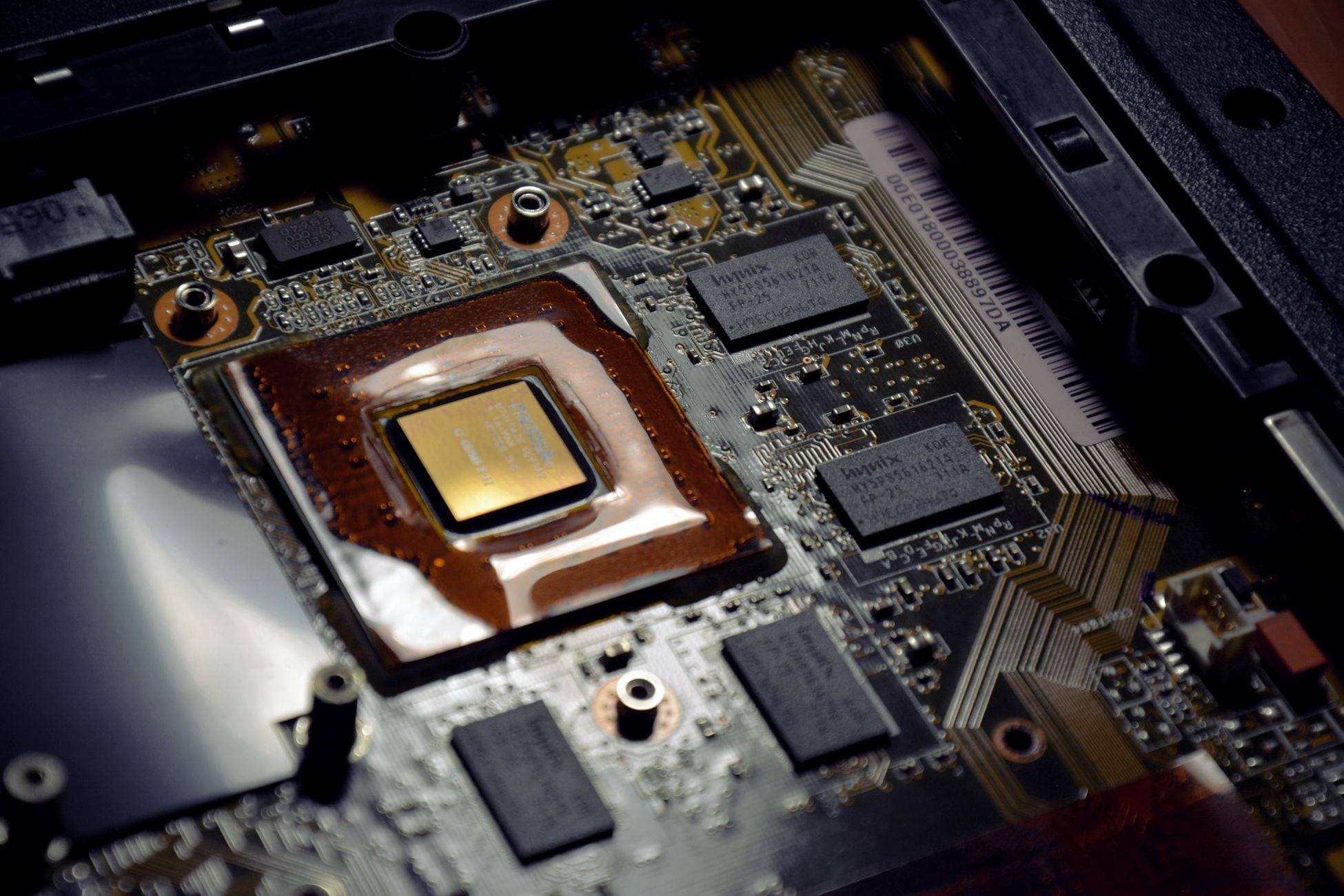
What a “product” actually is
When TSMC counts a product, it means a unique chip design taped out by a customer and run through a specific process node. An A-series Apple processor is one product. The slightly different variant binned for an iPad is another. A power management chip for a Bosch dishwasher is a third. A radar processor for a Volvo’s lane-keep system is a fourth.
That is how the number climbs into five digits. Each of those 12,682 designs has its own photomask set — the stack of quartz-and-chromium plates used to project circuit patterns onto silicon wafers. A single advanced mask set can cost upward of $20 million. Multiply by twelve thousand and the scale of capital sitting inside TSMC’s mask libraries starts to come into focus.
The 534 customers
The customer count is, in some ways, the more telling figure. Five hundred and thirty-four companies handed over their most sensitive intellectual property — the circuit designs that define their products — to a single manufacturer in 2025. Some of those customers are giants. Apple alone accounts for roughly a quarter of TSMC’s revenue. Nvidia, riding the AI boom, has become the second-largest single client.
The rest is a long tail of automotive suppliers, industrial sensor makers, medical device firms, defense contractors, and startups designing everything from hearing aids to satellite radios. SemiEngineering has described how European industries in particular have become accustomed to sourcing chips and subassemblies from Asian foundries almost by default — a habit formed when the rationale was purely about cost, and now stuck in place when the rationale has become about access.
Why a phone, a car, and a bank all end up at the same address
The iPhone 17’s A19 processor is fabricated at TSMC’s Fab 18 in the Southern Taiwan Science Park, on a 3-nanometer process. The Nvidia H100 GPUs running most of the world’s large language models come out of the same complex on a custom variant of the 4-nanometer node. The chips inside a modern car — and a vehicle contains roughly 1,400 to 3,500 semiconductors depending on the model — are spread across older nodes at TSMC fabs in Hsinchu and the company’s joint venture in Nanjing.
Even your bank card uses TSMC silicon. The secure elements made by NXP and Infineon, which authenticate contactless payments, are largely manufactured at TSMC’s mature 40nm and 28nm lines. Supply Chain Brain has documented how this concentration extends into public services — hospital scanners, traffic systems, water treatment controllers — all of which now depend on chips that trace back to the same handful of Taiwanese fabs.
The geography problem
Taiwan is roughly the size of the Netherlands. It sits approximately 130 kilometers off the coast of mainland China at the strait’s narrowest point, in a waterway that is one of the most heavily trafficked and politically contested in the world. The island generates more than 60 percent of the world’s foundry output and almost all of its leading-edge logic chips from an area smaller than Switzerland.
The fragility this creates is not theoretical. When CNBC reported in March 2026 on attacks affecting Qatar and the helium supply — a gas used to cool the lasers in extreme ultraviolet lithography machines — Asian tech stocks fell within hours. Helium comes from a few wells. EUV machines come from one company, ASML in the Netherlands. Advanced chips come from one foundry, TSMC. The chain has very few knots, and each of them is exposed.
What the 12,682 number replaced
In the 1990s, most large semiconductor companies were what the industry called integrated device manufacturers — Intel, Motorola, Texas Instruments, IBM, NEC. They designed their own chips and ran their own fabs. The economics worked because process nodes were cheaper to develop and the gap between leading-edge and trailing-edge was narrow.
That model collapsed under the cost of each new node. A modern 3nm fab costs more than $20 billion to build. Developing a process generation runs into the tens of billions more. Only a handful of companies in the world can afford to play, and TSMC’s founder Morris Chang built the pure-play foundry model — manufacturing for everyone, designing for no one — specifically to absorb that cost across hundreds of customers. IndustryWeek has argued that the model became so efficient it taught the rest of manufacturing the dangers of optimizing supply chains purely for cost.
► Watch · Silicon Canals The Island That Makes the World’s Brain Silicon Canals traces how the modern world quietly concentrated its entire technological foundation on one vulnerable island—and why no one can reverse it.

The Arizona and Kumamoto answer
The political response has been to try to spread the risk geographically. TSMC’s Fab 21 in Phoenix, Arizona, began limited production of 4nm chips in late 2024 and is ramping toward 3nm and eventually 2nm in subsequent phases. A second TSMC complex is operating in Kumamoto, Japan, focused on more mature nodes for the automotive and image-sensor industries. A planned fab in Dresden, Germany, is targeting industrial and automotive customers.
None of this dilutes the 12,682 figure in a meaningful way yet. The Arizona fab will produce a few dozen high-end designs at full capacity. The Kumamoto fab handles a similarly narrow slice. The vast majority of TSMC’s product mix — and almost all of its leading-edge work — remains in Taiwan, and is expected to remain there through at least the end of the decade.
What it means to depend on one company
The Apple Watch on a wrist in São Paulo, the ABS controller in a Renault in Lyon, the radar chip in a John Deere combine in Iowa, the AI inference card in a hyperscale data center in Dublin — all of them share an origin. Wafer started at a TSMC fab. Patterned by an ASML lithography machine. Diced, packaged, and shipped through a logistics network that converges on the same set of postal codes in Taiwan before fanning out across the globe.
Financial analysts have long flagged what they call the geopolitical overhang on TSMC’s stock — the persistent question of what happens to the world’s chip supply if anything disrupts operations on the island, even temporarily. The honest answer is that nobody knows, because nobody has ever tried to source 12,682 unique chip designs from somewhere else on short notice.
The number behind the number
There is a quieter figure inside the 12,682 that is worth sitting with. TSMC shipped roughly 16 million 12-inch equivalent wafers in 2025. Each wafer carries hundreds to tens of thousands of individual dies depending on the chip size. The total number of finished chips that left TSMC’s fabs last year runs into the trillions.
Trillions of small squares of patterned silicon, each one a customized product for one of 534 customers, each one carrying a circuit design that took years and millions of dollars to develop, each one passing through the same handful of buildings on the same island in the same strait. The supply chain of the modern world is, in one sense, a list of 534 names and a single address.
The chips inside the phone being read right now came from there. So did the chips routing the data to it.


-1024x683.jpg "AOC on the Warpath: Democrat Incumbents and Big Businesses Beware")


-1024x683.jpg "Florida Roads Become a Battleground for Illegal Immigration")


